New Generation
35kV / 5MW power electronic transformer
based on the 6.5kV / 400A SiC MOSFET / The 1st set of world
Comparing with conventional >>> Distribution transformer & Power Transformer & Cast Resin Transformer
New materials and new future
Silicon carbide (SiC) as a typical representative of wide belt semiconductor materials, breakdown high electric field, high thermal conductivity, high electronic saturation rate, strong radiation resistance, compared with the same structure of silicon devices, silicon carbide devices can reach 10 times the voltage, 4 times the current, 10 times the working frequency, high temperature resistance, using high voltage silicon carbide device can adopt new topology, greatly improve power density, reduce loss, support a new generation of power system advanced power electronic equipment development.
- The silicon carbide material has excellent performance
- Silicon carbide device has high pressure, high current, high current, high temperature resistance and other excellent characteristics
- Devices using silicon carbide devices can greatly increase the power density and reduce the loss
Full-chain technology breakthrough
For a new generation of power system core equipment technology demand, focusing on silicon carbide materials, device localization, project team for power electronic transformer technology demand task decomposition, developed each link, each level of research and development of detailed technical rules, specification, after multiple rounds of feedback iteration, through the high voltage high power silicon carbide MOSFET technology route, implements the material-chip-device-test-application validation whole technology chain collaborative innovation, promote the domestic high voltage high power silicon carbide materials, device industrialization, for power electronics device original innovation and international technology lead provides a strong support.
Marked results
The power Semiconductor Research Institute in the United Nations, the top technical force has opened the original technological innovation road of low defect density materials, high voltage high current chip, high voltage high capacity device packaging, high voltage fast switch test, new silicon carbide new system drive and the whole chain of transformers
Large size and low defect material
The performance, yield and cost of high voltage silicon carbide chip are greatly affected by the material quality. At the beginning of the project, there were no large size single crystal and no low defect thick epitaxial materials in China, which seriously restricted the independent research and development of high voltage and high current silicon carbide chip. Technical team for high pressure silicon carbide devices of epitaxial materials, epitaxial substrate material customization demand, temperature field control, stress control and release, thick epitaxial growth, low defect control technology research, overcome the high pressure silicon carbide devices for 6 inch single crystal substrate expansion growth, defect density control and large size epitaxial defect control, rapid epitaxial growth and other technical problems, developed the high quality domestic single crystal substrate, realize the low defect density thick epitaxial material preparation.
High-voltage and high-current chip
High-voltage module multi-chip parallel packaging puts forward higher requirements for the chip, high voltage, high current, good consistency. Project team based on the independent development of low defect thick epitaxial material, put forward the low surface field strength of high voltage chip terminal structure, overcome the high quality gate oxygen, short channel self-alignment technology and other key process, solve the design and process compatibility, conduction resistance, high debris rate, a series of problems, in the domestic first mastered the 6-inch silicon carbide chip process, domestic first batch developed high voltage resistance, high flow capacity of 6.5 kV / 25 A SiC MOSFET chip, through high temperature gate deviation, high temperature deviation series of reliability test. The chip technical indicators have reached the same level of international products, and some key indicators are better than the international similar devices.
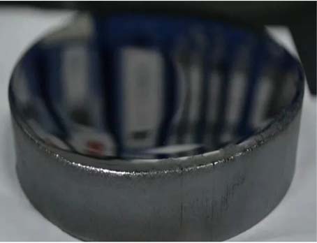
 6.5kV / 25A SiC MOSFET wafer
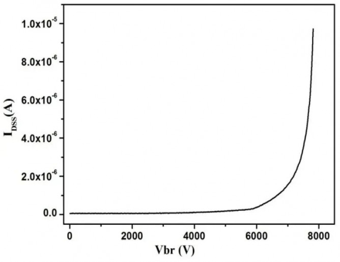
6.5kV / 25A SiC MOSFET blocking properties
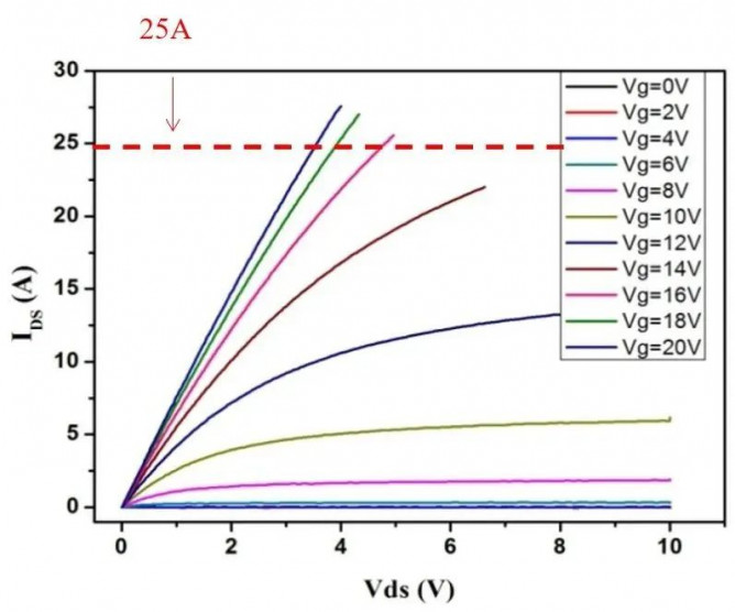
6.5kV / 25A SiC MOSFET output characteristics
High-voltage and high-capacity device packaging
High voltage and high capacity silicon carbide device packaging is faced with the difficulties of electromagnetic thermal equilibrium in parallel packaging, insulation coordination under high electric field strength, and silicon carbide packaging process is still in a blank state, The project team has developed high voltage insulation design, high thermal conductivity welding, high reliability insulation sealing and other core technologies, Breaking through the technical bottleneck of high pressure and low parasitic parameter packaging, We innovatively propose chip clustering grouping based on distance coefficient of transfer curve, Solve the problem of multi-chip parallel flow equalization faced by high-current packaging, The international same voltage level current maximum 6.5kV / 400A SiC MOSFET module has been successfully developed.
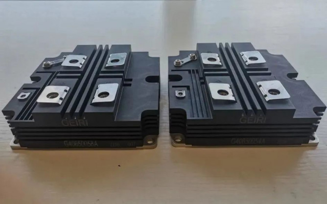
6.5kV / 400A SiC MOSFET module
Continuous operation test of 6.5kV / 400A SiC MOSFET device
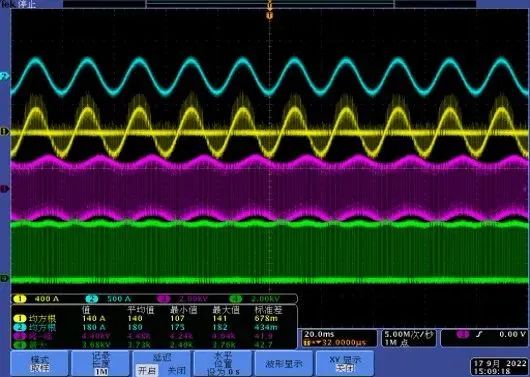
6.5kV / 400A SiC MOSFET device is continuous operation test waveform
High voltage Quick Switch test
The switching speed, drive voltage, parasitic diode characteristics and short-circuit characteristics of silicon carbide devices are significantly different from the silicon devices. The industry lacks special dynamic testing equipment for high-voltage and high-power silicon carbide devices, and there is no mature testing technology. In response to the typical conditions and extreme conditions, accurately evaluate the actual performance of devices, the technical team carried out the chip high precision test technology, module nanosecond level fast switch technology, high temperature gate oxygen performance evaluation technology research, built the first domestic a set of 6.5kV / 400A SiC MOSFET module dynamic test platform, low system parasitic parameters, overcome the shortcomings of the existing commercial test platform.
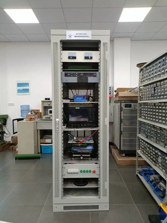
Self-developed dynamic testing platform of silicon carbide MOSFET device
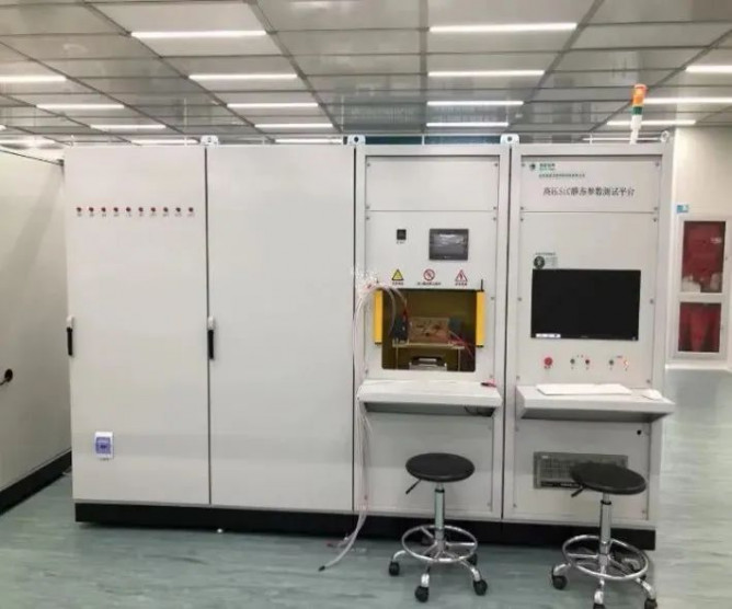
Self-developed 25kV / 4kA SiC device static testing platform
New silicon carbide system drive and transformer
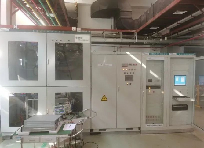
The brand-new power electronic transformer based on high-voltage silicon carbide devices needs technological breakthroughs in all aspects of topology, drive, control and protection, high-frequency and miniaturization. The technical team couples three power fluctuation single phase electromagnetic to realize power fluctuation self-balance, thus reducing the capacitor capacity value and even eliminating capacitor; develops the drive chip adapted to high-voltage silicon carbide device, gate drive voltage step control, through direct current detection, realize rapid protection of no blind field time; establish physical field simulation model of electromagnetic field, temperature field, stress field, realize good heat dissipation of high power density transformer through material and structure optimization of system shielding layer, water cooling design. Through the key technological breakthroughs such as high-speed drive and protection of high-voltage silicon carbide devices, high-performance control and protection of silicon carbide power electronic transformer, and integration test, the 35kV / 5MW full silicon carbide power electronic transformer was developed for the first time in the world and realized the demonstration application.
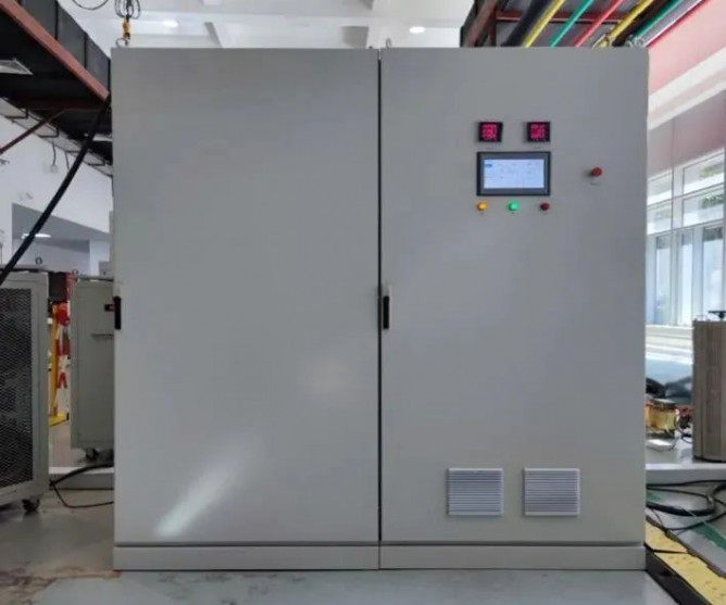
All-carbon silicon carbide power electronic transformer prototype
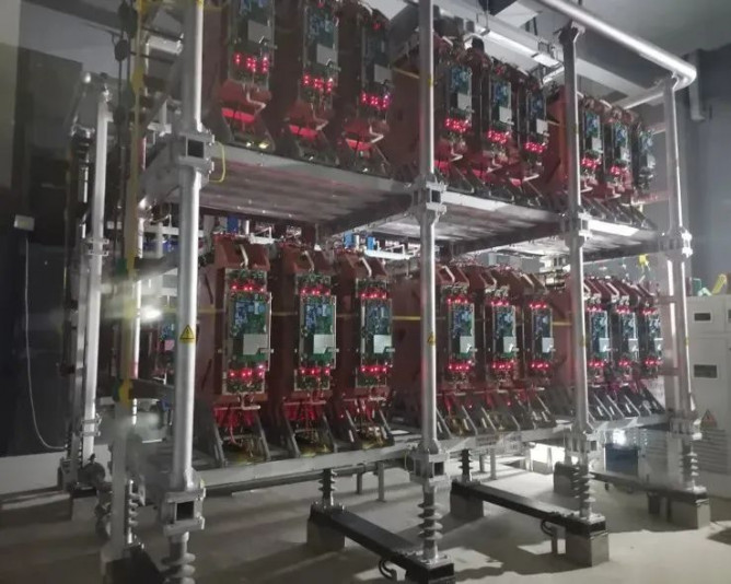
The silicon carbide power electronic transformer on the project site continues to operate stably
Learn more information about >>>> Prefabricated substation